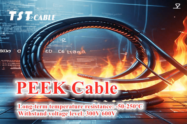

The semiconductor etching machine cavity is the “heart” of chip manufacturing, placing extremely stringent requirements on cable cleanliness, vacuum compatibility, plasma resistance, and high-frequency performance. TST CABLE PEEK cable solutions offer systematic, customized solutions specifically for the unique environment of etching processes.
I. Environmental Parameters and Challenges of the Etching Machine Chamber
1.1 Typical Etching Process Environment
| parameter | Typical value | Extreme values | Challenges to cables |
| vacuum degree | 10⁻⁵–10⁻⁷ Torr | 10⁻⁸ Torr | Low gas release, no volatile matter |
| plasma | 13.56 MHz RF | 2.45 GHz MW | Resistance to ion bombardment and carbonization |
| Process temperature | 25–150℃ | 200℃ | Thermal stability, dimensional stability |
| Etching gas | CF₄/SF₆/Cl₂/HBr/O₂ | Mixed gas | Resistant to strong corrosion and non-reactive |
| Particle control | <0.1 μm | <0.05 μm | Low particle precipitation |
| metal ions | <1 ppb | <0.1 ppb | Ultra-high purity |
| Gas release rate | TML < 0.1% | TML < 0.05% | Avoid cavity contamination |
| Dielectric constant | <3.2 | <3.0 | High-frequency signal integrity |
| Dielectric loss | <0.002 | <0.001 | Low signal attenuation |
1.2 Core Challenge Analysis
| Challenge Type | mechanism | Failure Mode | Solution direction |
| Plasma erosion | High-energy ion bombardment of PEEK surface | Carbonization, cracking, particle precipitation | Surface modification + nanofillers |
| Vacuum release | Release of volatiles from materials | Cavity contamination, decreased vacuum | Ultra-high purity materials + vacuum baking |
| High frequency loss | Dielectric loss + skin effect | Signal attenuation, mismatch | Low ε material + optimized structure |
| Chemical corrosion | Active free radical attack | Material degradation and performance deterioration | Selection of chemically inert materials |
| Particulate pollution | Surface wear/precipitation | Wafer defects and yield reduction | Ultra-smooth surface + clean process |
| Thermal expansion mismatch | Material CTE differences | Interface layering, connection failure | CTE matching design |
II. Custom Structural Design of TST CABLE PEEK Cable
2.1 Multi-layer protective structure (optimized for etching cavities)
Key structural parameters
| level | Material | thickness | Key features | Design basis |
| conductor | 5N high-purity silver-plated copper | According to signal requirements | Electrical conductivity ≥101% IACS, silver layer ≥2μm | SEMI F20 |
| Insulation layer | Ultra-high purity PEEK + 1.5% nano-SiO₂ | 0.3–0.6 mm | εᵣ≤2.9 (1 GHz), tanδ≤0.0008 | SEMI E122 |
| Inner sheath | Ultra-high purity PEEK (metal ions ≤ 0.1 ppb) | 0.15 mm | TML ≤ 0.05%, CVCM ≤ 0.005% | ASTM E595 |
| Shielding layer | Silver-plated copper braid (coverage ≥98%) | 0.12 mm | Shielding effectiveness ≥110 dB (1 GHz) | SEMI E179 |
| outer sheath | Ultra-high purity PEEK + 3% PTFE micro powder | 0.25–0.45 mm | Friction coefficient ≤ 0.15, particle precipitation ≤ 5 particles/cm² | SEMI F57 |
✅ Special Design:
Coaxial structure: used for RF signal lines, characteristic impedance 50±1 Ω
Double shielding layer: inner aluminum foil + outer braided layer, to withstand 2.45 GHz microwaves.
Surface polishing: outer diameter tolerance ±0.02 mm, Ra≤0.05 μm
III. In-depth optimization of material formulation
3.1 Precise Control of Nanofillers (High-Frequency Applications)
| filler | Added amount | Mechanism of action | Performance improvement | Risk control |
| Nano SiO₂ | 1–2 wt% | Reduce polar group density | εᵣ↓10%, tanδ↓15% | Distribute evenly to avoid clumping. |
| PTFE micro powder | 3–5 wt% | Reduce surface energy | Friction coefficient ↓50%, particle precipitation ↓ | Control particle size <0.5 μm |
| Nano Al₂O₃ | 0.5–1 wt% | Improve heat conduction channels | Thermal conductivity increases by 20%, heat accumulation decreases. | Avoid increasing dielectric loss |
| graphene | 0.1–0.3 wt% | Enhanced interface integration | Tensile strength increased by 15%, plasma resistance increased | Strictly control the amount added |
Key processes: Twin-screw extrusion + ultrasonic dispersion to ensure uniform distribution of nanofillers (SEM verification)
3.2 Conductor Coating Optimization Scheme
| Application scenarios | Recommended coating | thickness | Advantages | Cost coefficient |
| High-frequency RF signal (13.56 MHz) | silver | 2–3 μm | Low skin effect, high conductivity | 1.0× |
| Microwave signal (2.45 GHz) | Gold plating | 1–2 μm | Excellent oxidation resistance, low contact resistance | 3.0× |
| Heater power supply | Nickel plating | 3–5 μm | High temperature resistance, moderate cost | 0.8× |
| Sensor signals | silver | 2 μm | Balancing performance and cost | 1.0× |
IV. Cleanroom Manufacturing Process Control
4.1 Cleanliness control throughout the entire process
| Link | cleanliness | Key control measures | Verification method |
| Raw material storage | ISO Class 5 | Nitrogen holder, humidity <30% RH | Particle counter |
| Extrusion workshop | ISO Class 6 | Positive pressure + HEPA filter, cleanroom suits for personnel | Settling bacteria test |
| Weaving workshop | ISO Class 6 | Antistatic flooring, ionizer | Electrostatic test |
| Finished product packaging | ISO Class 5 | Nitrogen-filled, double-layer vacuum bag | Residual oxygen detection |
| Transport and storage | ISO Class 7 | Dedicated cleanroom box, temperature and humidity recording. | Transportation verification |
4.2 Key process parameters (specific to etching chamber)
| Process | parameter | Control precision | Verification method |
| conductor stranding | Pitch/Outer Diameter ≤ 8 | Tension fluctuation ≤3% | Microscope + Tensiometer |
| Insulation extrusion | Temperature 375±2℃ | Vacuum degree ≤3 Pa | Eccentricity meter + vacuum gauge |
| Nanodispersion | Shear rate 180 s⁻¹ | Temperature fluctuation ≤1℃ | SEM observation |
| Shielding braid | Coverage ≥ 98% | Tension control ±2% | Microscopic examination |
| Outer sheath extrusion | Temperature 365±2℃ | Controllable cooling rate | Size measurement |
| Vacuum baking | 150℃×72h | Vacuum degree ≤10⁻³ Pa | TGA verification |
4.3 Key Quality Control Points (Semiconductor Grade)
| Control Points | Testing items | frequency | Qualification Standard | Testing equipment |
| Incoming material inspection | Metal ions (ICP-MS) | Each batch | ≤0.1 ppb | ICP-MS |
| Particle detection | Surface particles (>0.1 μm) | Each batch | ≤5 pieces/cm² | Laser Particle Counter |
| Process control | Insulation thickness eccentricity | 100% online | ≤6% | Laser diameter measuring instrument |
| Spark test | Insulation defects | 100% | 15 kV No breakdown | EDM |
| High frequency test | εᵣ, tanδ(1 GHz) | Each batch | εᵣ≤2.9, tanδ≤0.0008 | Vector Network Analyzer |
| Gas release test | TML, CVCM | Each batch | TML ≤ 0.05%, CVCM ≤ 0.005% | Vacuum gas release test stand |
| cleanliness | Metal residues (ICP-MS) | Each batch | Total metals ≤ 0.5 ppb | ICP-MS |
V. Etching Cavity Environment Testing and Verification Plan
5.1 Vacuum release test (ASTM E595 + RGA)
| Test Project | condition | Qualification Standard | Equipment Requirements |
| TML | 125℃×24h, 10⁻⁵ Torr | ≤0.05% | Vacuum release test stand |
| CVCM | Same as above | ≤0.005% | Cold finger collection device |
| WVR | Same as above | ≤0.05% | Moisture analyzer |
| RGA analysis | Real-time monitoring of vacuum chamber | No abnormal C/H/F/O peaks | Residual Gas Analyzer |
✅ Additional requirement: No visible deposits on the cable surface after testing (verified by optical microscopy)
5.2 Plasma tolerance test (SEMI F57 + custom)
| Test Project | condition | Qualification Standard | Verification method |
| CF₄ Plasma | 300 W, 50 mTorr, 2h | Weight loss ≤0.5%, no carbonization | SEM + Weight Analysis |
| Cl₂ plasma | 200 W, 40 mTorr, 2h | Surface is free of corrosion, and εᵣ change is ≤5%. | XPS+ Dielectric Testing |
| HBr/O₂ plasma | 250 W, 45 mTorr, 2h | Particle precipitation ≤3/cm² | Particle counter |
| Mixed gas | CF₄/Cl₂/O₂, 3h | Stable overall performance | Full parameter testing |
| Long-term exposure | Actual process conditions × 100h | No function failure | Equipment vendor verification |
5.3 High-frequency performance testing (SEMI E122/E179)
| Test Project | Frequency range | Qualification Standard | Test equipment |
| Dielectric constant (εᵣ) | 1 MHz–10 GHz | ≤2.9 (1 GHz) | Vector Network Analyzer |
| Dielectric loss (tanδ) | 1 MHz–10 GHz | ≤0.0008 (1 GHz) | Same as above |
| Characteristic impedance | 100 MHz | 50±1 Ω | TDR Time Domain Reflectometer |
| VSWR | 13.56 MHz–2.45 GHz | ≤1.15 | Vector Network Analyzer |
| Insertion loss | 1 GHz | ≤0.3 dB/m | Vector Network Analyzer |
| Shielding effectiveness | 10 MHz–10 GHz | ≥110 dB | Shielding effectiveness testing system |
5.4 Chemical and Cleanliness Testing
| Test Project | condition | Qualification Standard | standard |
| CF₄ gas immersion | 100℃×168h | Weight change ≤0.5%, strength retention ≥95% | ASTM D543 |
| Cl₂ gas immersion | 80℃×168h | Non-corrosive and with stable dielectric properties | ASTM D543 |
| SC1/SC2 cleaning | Room temperature × 24h | No swelling, no cracking | SEMI C33 |
| Particle precipitation | Ultrapure water rinsing | >0.1 μm particles ≤3 per cm² | SEMI F21 |
| metal ions | ICP-MS analysis | Total metals ≤ 0.5 ppb | SEMI F20 |
| Organic residues | GC-MS analysis | ≤0.5 ppb | SEMI F33 |
| Surface roughness | Atomic force microscope | Ra≤0.05 μm | SEMI E179 |
VI. Certification and Standards System
6.1 List of Required Certifications
| Authentication type | Certification bodies | Validity period | Key Requirements |
| SEMI F57 | SEMI | long | plasma tolerance |
| SEMI F20 | SEMI | long | Metal impurity control |
| SEMI E122 | SEMI | long | High frequency performance |
| SEMI E179 | SEMI | long | Size and Electrical |
| SEMI F21 | SEMI | long | Particle precipitation |
| ISO 14644-1 | ISO | 3 years | Cleanroom Certification |
| RoHS/REACH | SGS/TUV | long | Environmental compliance |
6.2 Equipment Vendor-Specific Requirements (Reference)
| Equipment vendor | Special requirements | Verification method |
| Applied Materials (AMAT) | Particle precipitation ≤ 2 particles/cm² | Customer Lab Validation |
| Lam Research Institute | Mixed gas plasma 100h | Customer on-site testing |
| Tokyo Electron (TEL) | Metal ions ≤ 0.3 ppb | ICP-MS Report |
| AMEC (Advanced Micro-Fabrication Equipment Inc.) | Domestic production rate ≥ 70% | Supply chain audit |
VII. Supplier Selection and Cooperation Strategy
7.1 Core Qualification Requirements for Suppliers
| Qualifications | Require | Verification method |
| SEMI Certification | F57/F20/E122/E179 complete | Certificate Inquiry |
| cleanroom | ISO Class 5-6, with operational records. | On-site audit |
| Success stories | ≥3 mainstream etching equipment manufacturers supply | Customer testimonials |
| Testing capabilities | Own vacuum release + plasma testing station | Laboratory audit |
| Quality System | ISO 9001 + ISO 14644-1 | Certificate verification |
| R&D team | Semiconductor Materials Special Project ≥ 8 people | Team Introduction |
VIII. Installation, Operation and Maintenance and Failure Prevention
8.1 Key Points for Cavity Installation
| Link | Precautions | Risk avoidance |
| Transport and storage | Nitrogen packaging, avoid direct sunlight. | Prevents contamination and moisture absorption |
| Cavity through the wall | Dedicated vacuum feedthrough (metal seal) | Prevent leakage (<1×10⁻⁹ Pa·m³/s) |
| Curved laying | Minimum bending radius ≥ 12 × D | Prevent insulation damage |
| Fixing method | Dust-free PEEK clips prevent metal contact. | Preventing particulate pollution |
| Terminal connection | Special torque wrench with torque control | Prevent poor contact |
| Shielding grounding | Single-point grounding, grounding resistance <0.01Ω | Prevent RF interference |
8.2 Operation and Maintenance Monitoring and Lifecycle Management
| Monitoring Projects | Monitoring cycle | Warning threshold | Handling measures |
| vacuum degree | real time | Abnormally high >10% | Inspect the source of the leak |
| RF matching | Each process | VSWR>1.3 | Check cable condition |
| Signal quality | per month | Attenuation increase >0.2 dB | Evaluation and replacement |
| Visual inspection | Each PM | Discoloration/Carbonization/Particles | Replace immediately |
| Particle monitoring | Each PM | Abnormal increase in cavity particles | Inspect cable contamination |
| Preventive replacement | By process hours | Cumulative plasma exposure >5000h | Planned replacement |
8.3 Common Failure Modes and Prevention
| Failure Mode | root cause | Preventive measures |
| Surface carbonization | High plasma energy + material mismatch | Optimize materials + reduce power density |
| Particulate pollution | Surface wear + insufficient cleanliness | Ultra-smooth surface + PTFE micro powder |
| Signal mismatch | Dielectric degradation + loose connection | Regular VSWR monitoring + torque control |
| Vacuum leak | Feedthrough seal failure | Metal seal + helium leak detection |
| Metal pollution | Excessive metal ions in materials | Ultra-high purity materials + ICP-MS verification |
| thermal damage | Poor heat dissipation + heat accumulation | Optimized structure + added thermally conductive filler |
IX. Cost and Delivery Cycle
9.1 Cost Structure Analysis (High-End Etching Machine Applications)
| Cost items | percentage | illustrate |
| Material costs | 55–65% | Ultra-high purity PEEK + nanofiller + 5N copper |
| Clean manufacturing | 15–20% | Cleanroom + Special Process |
| Testing and Certification | 10–15% | Vacuum release + plasma + high frequency testing |
| Research and development amortization | 5–10% | Custom development costs |
| Management and Profit | 5–10% | Reasonable profit margin |
Reference Price:
High-end imported (Gore/LEONI): 2500–4500 RMB/meter
Japanese brand (Mitsubishi): 1800–3000 RMB/meter
Domestic high-end (Zhongtian/Hengtong): 1000–2000 RMB/meter
Domestic standard: 600–1200 yuan/meter
9.2 Delivery cycle (from launch to volume delivery)
| stage | cycle | critical dependencies |
| Requirements definition + design | 3–6 weeks | Equipment vendor technical specifications acquisition |
| Sample Development | 6–10 weeks | Cleanroom scheduling |
| Environmental testing | 10–14 weeks | Laboratory scheduling (plasma testing takes the longest). |
| Equipment vendor verification | 4–8 weeks | Customer lab availability |
| Certification application | 4–8 weeks | SEMI Certification Process |
| Mass production | 3–6 weeks | Raw material stockpiling |
| total | 30–48 weeks | It is recommended to allow a buffer period. |
⚠️ Key Note: Plasma testing and equipment vendor verification is the longest process; it is recommended to book laboratory resources in advance.
10. Recommendations for Customization in Special Application Scenarios
10.1 High-Frequency RF Applications (13.56 MHz / 2.45 GHz)
| Customization points | Technical solution | Validation requirements |
| conductor | 5N silver-plated copper, 40 strands x 0.1 mm fine twist | Skin depth calculation verification |
| insulation | Nano-SiO₂ modified PEEK, εᵣ≤2.8 | At 1 GHz, εᵣ≤2.8 |
| shield | Double-layered (aluminum foil + silver-plated braided fabric), with a coverage of ≥99%. | 110 dB@1 GHz |
| structure | Precision coaxial, outer diameter tolerance ±0.02 mm | VSWR≤ mailto:1.15@2.45 GHz |
| test | Full-band S-parameters, phase stability | Phase jitter ≤2° |
1 0 2 Ultra-high vacuum applications (<10⁻⁸ Torr)
| Customization points | Technical solution | Validation requirements |
| Material | Ultra-high purity PEEK (TML≤0.03%, CVCM≤0.003%) | RGA has no C/H/F peaks |
| process | Vacuum baking (150℃×96h) + nitrogen sealing | TML retest after baking |
| Package | Double-layer vacuum bag + nitrogen filling, residual oxygen <10 ppm | Packaging integrity verification |
| test | 10⁻⁸ Torr environment gas release test | The vacuum level stabilized after 24 hours. |
1 0. 3 Multi-gas compatible applications (CF₄/Cl₂/HBr/O₂ mixture)
| Customization points | Technical solution | Validation requirements |
| outer sheath | PEEK/PTFE blend (65/35) + nano Al₂O₃ | Mixed gas plasma 100h |
| test | Actual process gas ratio, 300 W × 5h | Weight loss ≤1%, no carbonization |
| verify | Equipment vendor on-site process verification | No abnormalities after 1000 hours of continuous operation |
Cleanliness and precision: the lifeline of semiconductor manufacturing
Customizing PEEK cables for semiconductor etching machine cavities
is not “cable manufacturing,” but rather “process extension.”
TST CABLE PEek cable manufacturing core principles:
✅ Cleanliness First: 0.1 ppb metal control, 0.05 μm particle limit
✅ Data-Driven: Every performance indicator must be supported by SEMI standard test data
✅ Certification Closed Loop: Dual guarantee of SEMI certification + equipment manufacturer certification
✅ Full Life Cycle: Reliability management throughout the entire process from design to decommissioning
TST CABLE recommends:
forming a cross-functional team (process + materials + equipment + quality),
adopting a joint development model (deep supplier involvement),
verifying and iterating in stages (sample → testing → field → mass production),
and establishing long-term strategic cooperation (technology sharing + continuous optimization) –
because behind every meter of cable
lies a solemn commitment to the yield of nanometer-level chips.
TST CABLE recommends:
Clarify your etching process details (gas formulation, power, frequency, equipment model)
, contact SEMI-certified suppliers for technical discussions,
initiate small-batch sample development and testing,
and simultaneously communicate certification requirements with equipment manufacturers.
For further refinement of technical parameters, supplier recommendations, or customized testing solutions, TST CABLE can provide professional support.
Cleanliness is of utmost importance; precision determines success or failure.
Also available in:
![]() English
English